

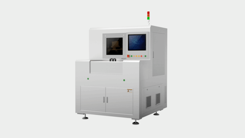
The fast-paced development of micro-electronics and semiconductor manufacturing has dramatically changed the standards of production. With the shrinking size of electronic devices but an increase in computing density, producers are now faced with the new task of how to mark, trace and identify micro-level parts without damaging their structure or functionality.
The traditional methods of marking, such as thermal fiber lasers, CO2 processing, or continuous inkjet printing, do not perform well in the electronic systems with high density. Heat-affected zones (HAZ) may lead to microcracks in thin silicon wafers, combustion of circuit board bases, or weakening of fragile polymeric packing. To avoid these issues, the micro-electronics industry adopted ultraviolet (UV) laser technologies as a modern standard of material treatment.
The Physics Behind Cold Processing: Why UV Lasers Excel:
The primary reason for UV laser technology’s success is its very short wavelength of 355 nm. Infrared lasers like fiber or CO2 lasers operate in the infrared spectrum where thermal energy is used to melt or ignite or vaporize the surface material.
However, UV laser works by photochemical ablation, which is what industrial engineering refers to as “cold processing”. Rather than generating excessive heat, high-energy photons from UV lasers are used to disrupt the molecular bonding in the material being targeted.
There are a few important advantages of using this technology in microelectronics:
- Minimal heat affected zone: UV laser processing minimizes heat input and the heat-affected zone, helping reduce the risk of micro-cracking, melting, discoloration, or warping.
- Micro-spot focusability: The 355 nm wavelength laser can create extremely small spot sizes (usually no bigger than 10-15 microns).
- Great material absorption: Almost all types of materials (plastics, semiconductors, silicon wafers, glass, metals) absorb the laser light and can be modified without causing any damage. damage-free surface modification.
Precision Applications in Micro-Electronics and Semiconductors:
1. Integrated Circuit (IC) and Chip Packaging:
Microchips and IC packages need clear serialization, 2D Data Matrix codes, and brand logos to enable supply chain traceability and prevent counterfeiting. Today’s semiconductor encapsulation materials, such as epoxy molding compounds or delicate resin housing, are highly susceptible to thermal stress. Using precision UV laser marking machines can produce high-visibility permanent tracking marks on the chip surface with low thermal impact when suitable parameters are used.
- Printed Circuit Boards (PCB and FPC):
With the rise of High-Density Interconnect (HDI) boards and Flexible Printed Circuits (FPCs) in modern smart devices, it has become necessary to mark lines at micro-meter levels. The conventional method of mechanical or thermal marking can cause damage to the thin copper wires or change the shape of the very thin circuit boards. The use of UV laser technology is able to engrave barcodes and component identification on the solder masks, substrates made of FR-4, and flexible circuits with millimeter readability.
3. Semiconductor Wafer Traceability:
Tracking of the wafer level is an important task for the manufacturers of semiconductors who are performing high-yield operations. Manufacturers can use laser marking for wafer and substrate traceability on materials such as silicon and sapphire. SEMI standards define marking and traceability requirements, while the specific laser wavelength and process parameters depend on the application.
4. Miniaturized Electronic Components:
A variety of electronic elements like connectors, SMDs, micro-relays, and medical sensors require high-quality identification within very limited space, just a few millimeters. The ultra-small spot size of UV laser systems makes it possible to engrave micro-text as tiny as 0.1 mm with high legibility.
Strategic Advantages in Modern Automated Manufacturing:
Getting the UV laser printing technique brings concrete and professionally beneficial results to high-tech production companies:
- Zero Consumables: Contrary to ink-jet printing, UV laser systems do not need inks, solvents, or chemicals. As a result, continuous chemical expenses are eliminated, equipment care is reduced, and green manufacturing rules are observed (RoHS compatible).
- Permanent Traceability: Laser marking keeps its quality regardless of the high temperature and strong industrial processes, which guarantees product tracking forever.
- Automated Line Integration: Available in a number of variants—compact 5W table-top versions and enclosed 10W and 15W industrial systems—UV systems are easily integrated into fast SMT assembly lines and vision-guided “pick-and-place” robots.
Future Outlook: The Next Phase of Micro-Scale Precision:
Today consumer technology is moving deeper into 3nm chip designs, flexible wearables and advanced automotive micro‑controllers. I notice that the space for manufacturing mistakes keeps getting smaller. Thermal processing is quickly being replaced by optical tools, in high‑precision supply chains.
Because UV laser technology gives high photon energy, cold processing dynamics and extreme focal accuracy UV laser has moved from a niche tool to an asset. For micro‑electronics manufacturers who want to improve yields, keep quality control and future‑proof their assembly lines, UV laser precision is the final advantage.
